Lolin32 Lite (ESP32) 8MB PSRAM Upgrade Mod

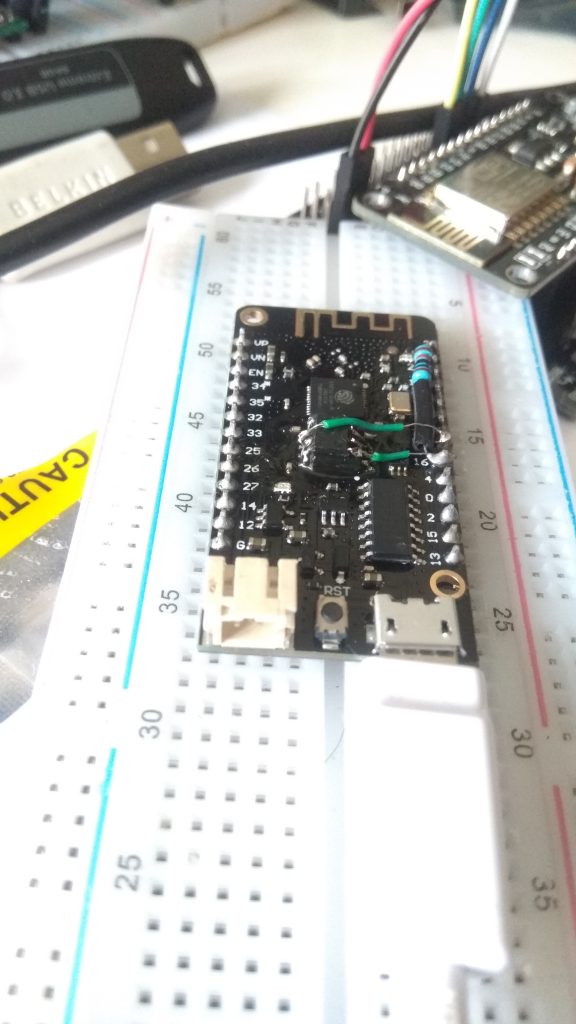
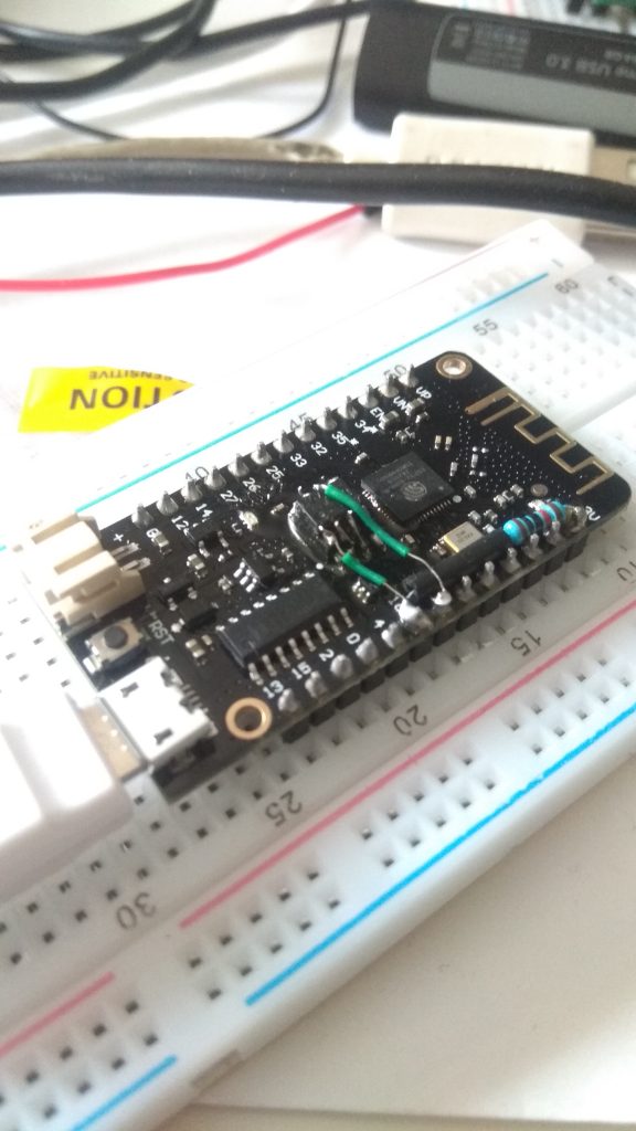
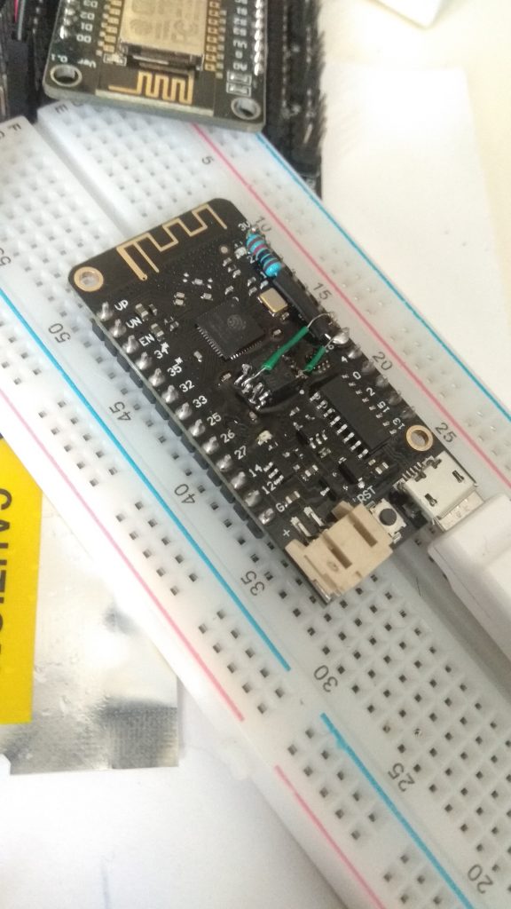
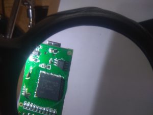
By piggybacking a PSRAM chip on to the existing flash chip we can get a whopping additional 8MB of addressable RAM.

Pseudostatic RAM (AKA PSRAM) as described on Wikipedia is, in short,

PSRAM or PSDRAM is dynamic RAM with built-in refresh and address-control circuitry to make it behave similarly to static RAM (SRAM). It combines the high density of DRAM with the ease of use of true SRAM.

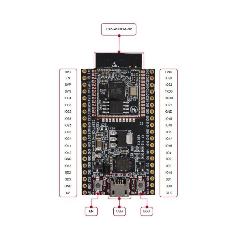
The WROOM-32 based ESP32 development boards are quite versatile but they are lacking PSRAM as standard. Whereas the newer WROVER boards ship with PSRAM as the norm and is typically 4MB (megabytes) in size, but the WROVER based development boards are unfortunately almost double the cost of the WROOM-32 based development boards.

Laboris documented a successful upgrade of a ESP-WROOM-32 @ Info Upgrade ESP32 board without psRAM with 4MB/8MB SPIRAM

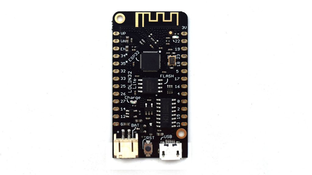
Sooooo, having a bunch of Lolin32 Lites at hand and a bunch of newly acquired IPUS IPS6404L-SQ SPI/QPI PSRAM, I thereby decided to give it a go. Not willing to wait until my 16MB (megabyte) flash chips arrived – my original plan was to replace them as well, which would have given a grand total of 16MB Flash/8MB PSRAM plus the original 520KB of internal SRAM, but alas impatience got the better of me and I hastily forged ahead keeping the original 4MB of flash in place.

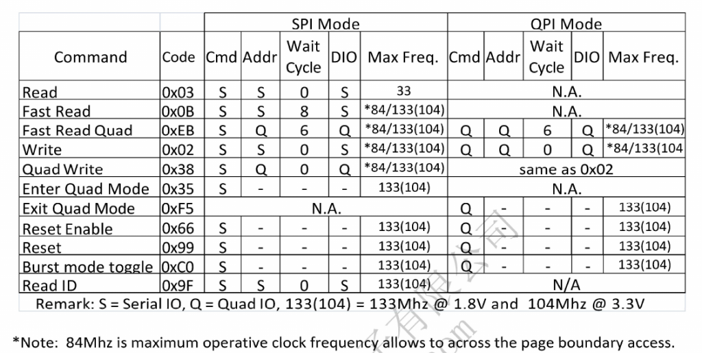
The IPS6404L-SQ PSRAM datasheet

specifies that the PSRAM is available as a 1.8v or a 3.3v variant.

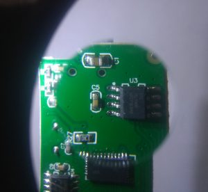
By way of flash storage the Lolin32 Lite uses the 32Mbit (4MB) 3V Winbond W25Q32JVSSIG (datasheet, click here)

and as the plan was to piggyback the PSRAM directly on to the back of the Winbond flash chip, I would need to use the matching 3V part, namely the IPS6404L-SQ-SPN version of the PSRAM and luckily that is what I have to hand, 48 of them @ £0.60 each, which per unit is actually cheaper than a 23lc1024-i/sn 1024Kbit SPIRAM part, and yes you can use the PSRAM as box standard SPIRAM.

Piggybacking an IC does mean having access to it (the IC), and the Lolin32 Lite, by not using a WROOM-32 module and having a custom design (unlike the DevkitC), has all the ICs exposed (and hence the reason I use them). Actually if you dismantled and piggybacked a WROOM-32 module you wouldn’t be able to refit the Can.

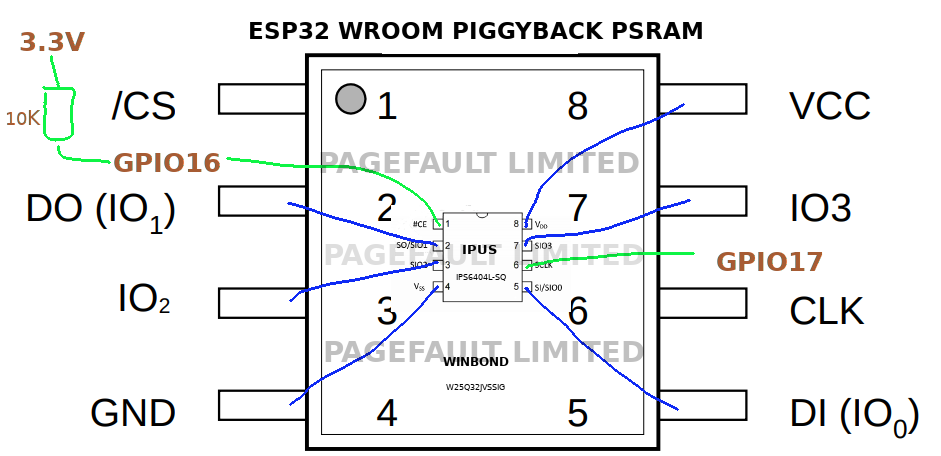
To perform the piggyback, just place the PSRAM on top of the Flash chip, in the correct orientation (i.e. Pin 1 to Pin 1, Pin 8 to Pin 8) and solder all pins excepting –

  • Pin 1 – CE/CS
  • Pin 6 – SCK

Pins 1, 6 and the 10K pull up are specific to the PSRAM (and the flash which has its own pin 1,pin 6 and resister pullup) and allow the two devices to be controlled individually.

  • Pin 1 should be wired to GPIO16 and provides the Chip Select for the PSRAM.
  • Pin 6 should be wired to GPIO17 and provides the SCLK for the PSRAM.
  • GPIO16 should be pulled up to 3V via a 10K resistor to ensure that the PSRAM is deselected during boot up.

NOTE: GPIO16 and GPIO17 will no longer be available for normal use after fitting the the PSRAM!!! Yes you just lost two pins!

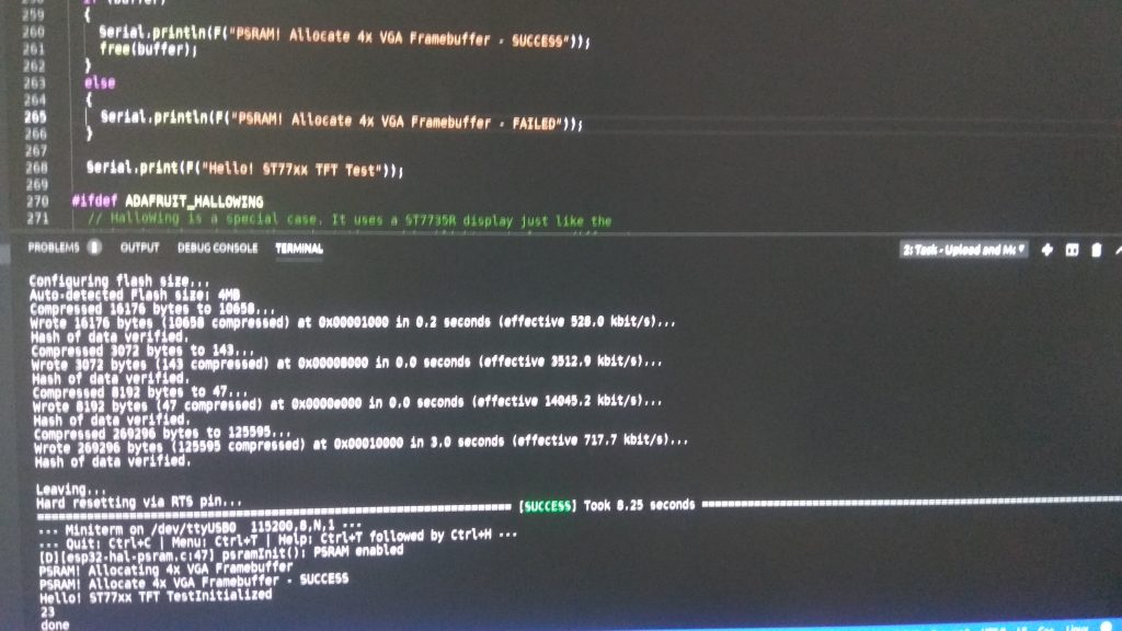
As to enabling the PSRAM in PlatformIO, all that is required is to simply add the following PSRAM related build defines to your “platformio.ini” file.

After which you should hopefully see a message saying “PSRAM enabled”

Assuming that your PSRAM is enabled and active, you will now be able to use 4MB of the 8MB PSRAM as normal addressable memory, which you can subsequently allocate and use with the “ps_malloc” function.

What about the remaining 4MB, I hear you say, well the remaining 4MB of the 8MB PSRAM is accessible using the ESP32 High mem Allocation API,
a form of bank switching, where sections of ram are mapped in and out of the same address space, all of which takes me back to the good old bank switching days of Commodore 128s and Atari 130XEs, but I digress. An example doing a simple memory test of the high memory range is available at esp-idf: system/himem

Links

ESP32-IDF: Support for external RAM

Hotchip – HT4928S Ver1.1 English PDF

The Hotchip HT4928S english datasheet

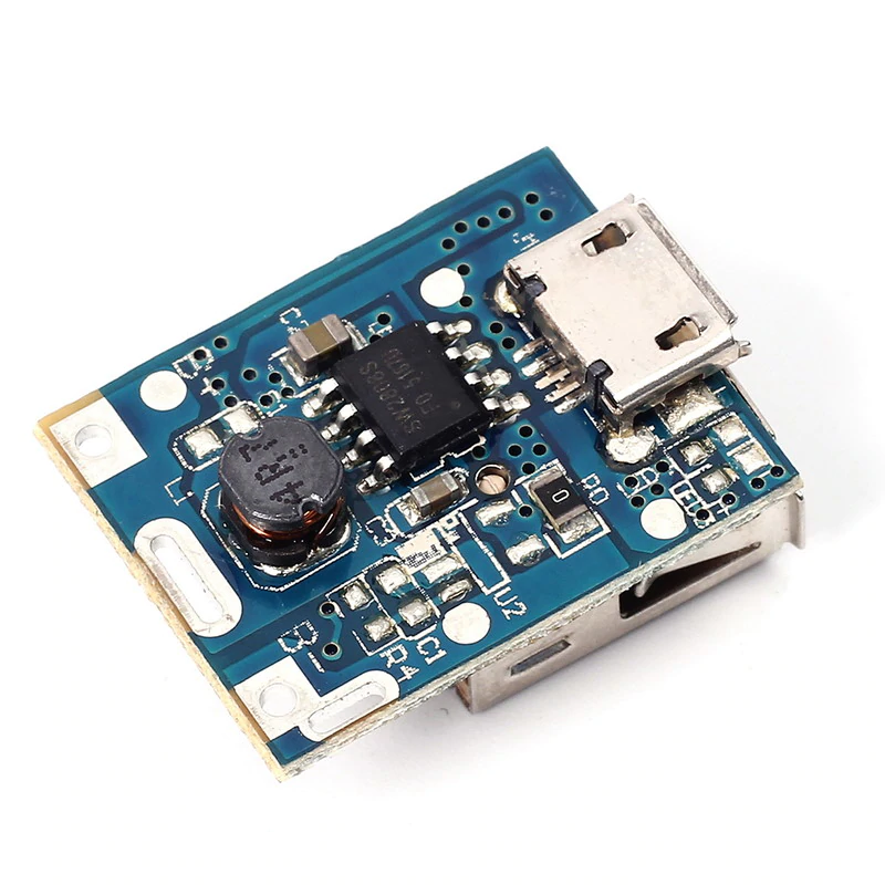
The HT4928S is a highly integrated mobile power supply Management chip with a built-in charge management module, an LED indicator Block, a boost discharge management module and is available in a small SOP8 Package. The periphery can be composed of very few components for a powerful mobile power solution.

It may or may not be the management chip that is on this module, described on Aliexpress as “5V-Step-Up-Power-Module-Lithium-Battery-Charging-Protection-Board-Boost-Converter-LED-Display-USB

With more than a little help from Google Translate, I translated the Chinese HT4928S datasheet

to English. Enjoy!

Wemos Lolin32 Pinout vs Wemos Lolin32 Lite Pinout

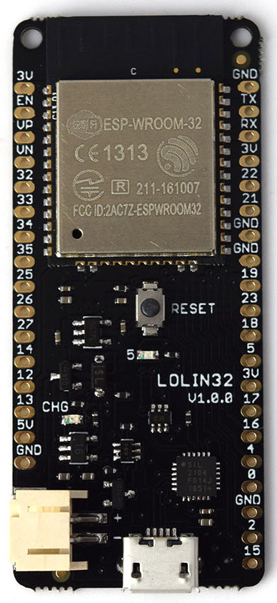
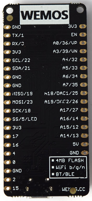
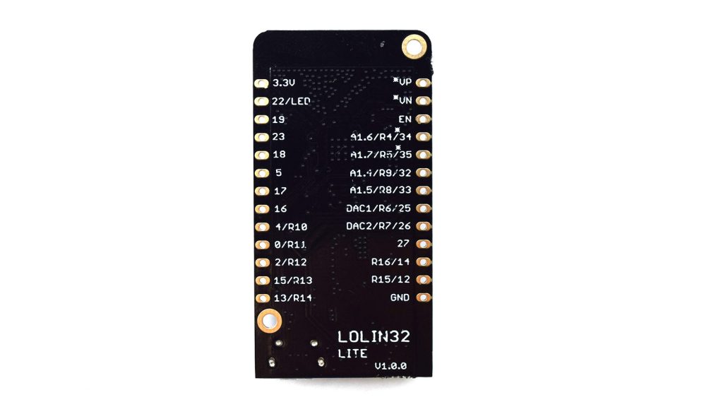
A complete Wemos Lolin32 Pinout Diagram showing all alternate functions in full.

Not being able to find a complete pinout diagram for the ESP32 based Wemos Lolin32, I decided to create one. I have included an existing pinout of the Wemos Lolin32 Lite too, for comparison purposes between the two boards.

Enjoy! click to view

.

Product Page

Wemos Lolin32 – https://wiki.wemos.cc/products:lolin32:lolin32

Wemos Lolin32 Lite – https://wiki.wemos.cc/products:lolin32:lolin32_lite

Adding Digital Channels to the DSO-150 Oscilloscope And Flashing New Firmware

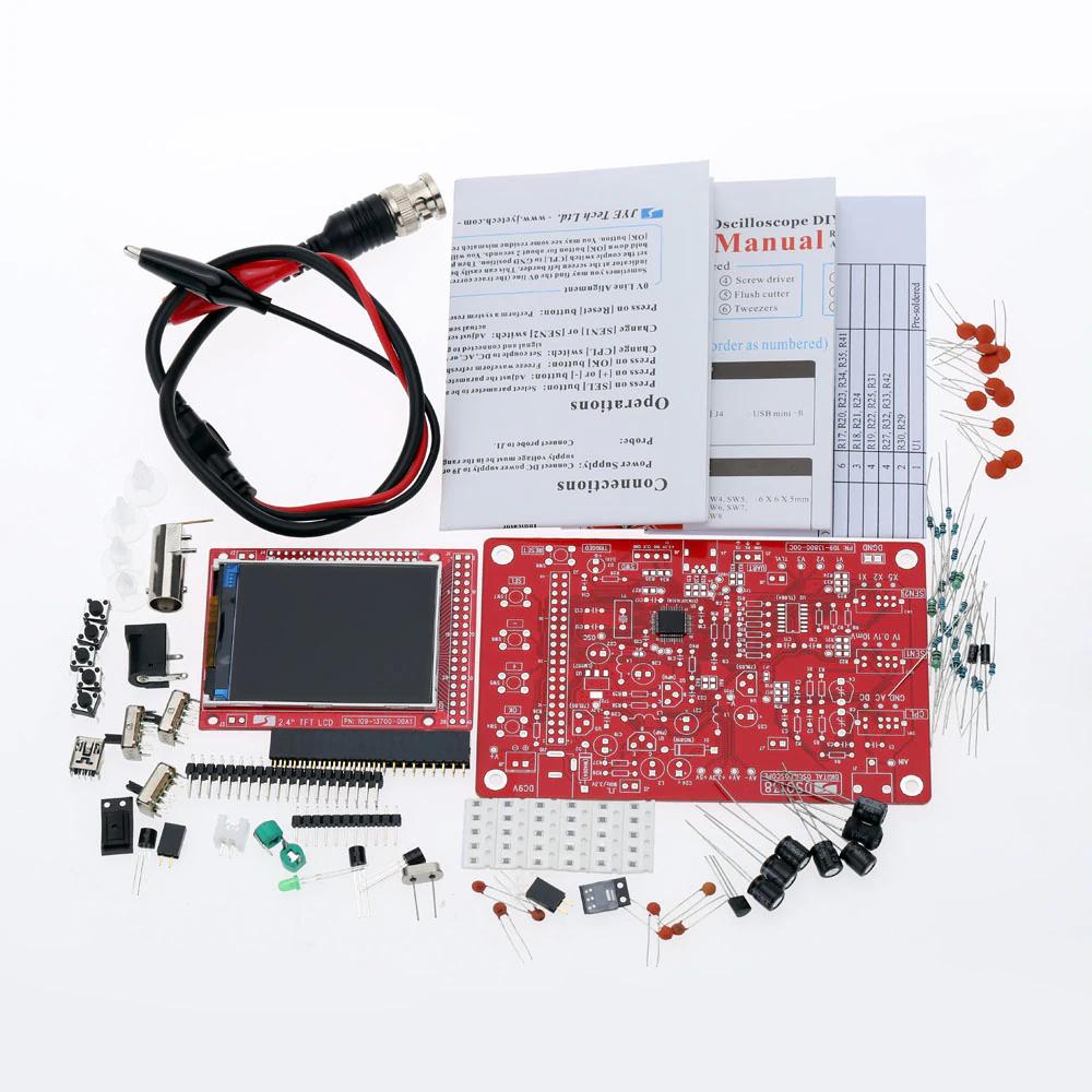
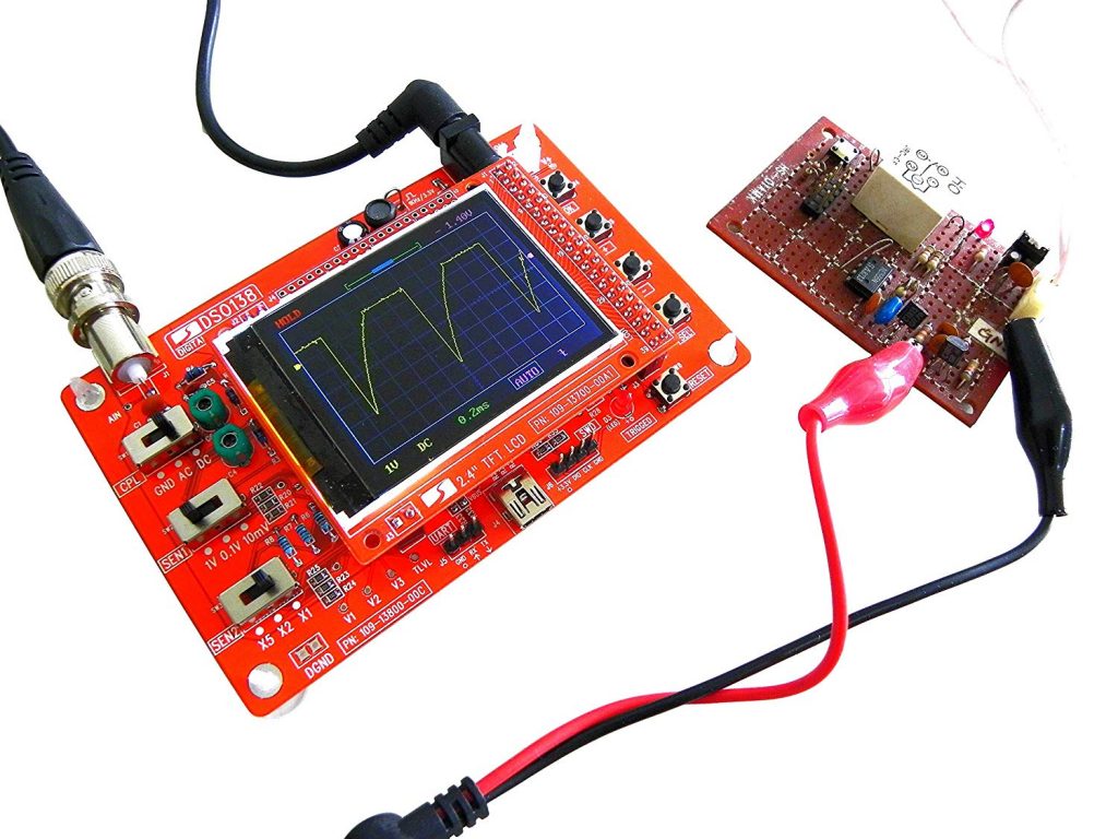
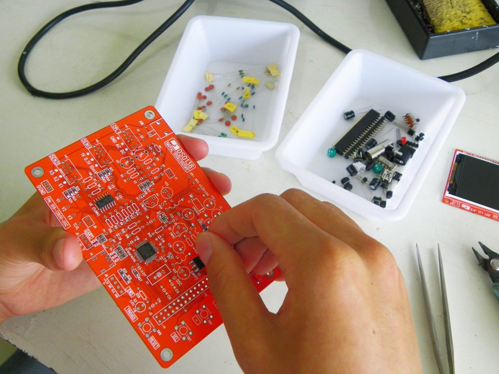
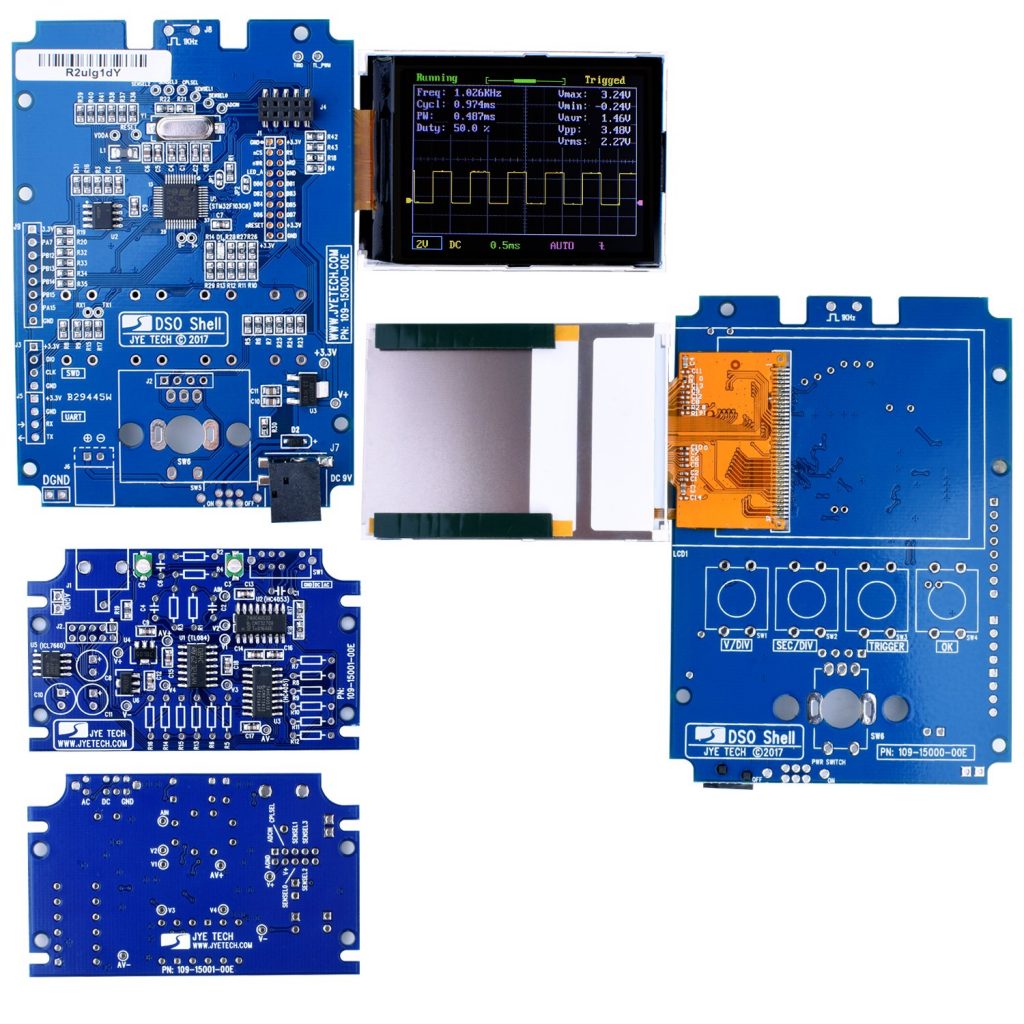
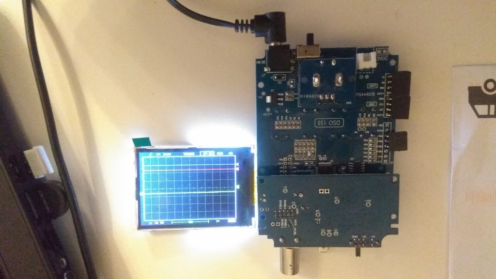
For some time I have been aware of the little portable oscilloscopes (DSO) kits produced by JYE Tech, such as the DSO-138 and DSO-150. While these kits can be purchased fully built, they are usually sold in a DIY state of “you solder everything” or “you solder everything minus the smd components”. In the images below, the red PCB is the DSO-138 and the blue PCB is the big brother DSO-150.

I required a portable oscilloscope for some analog related projects, but I also wanted the ability to capture digital output at the same time. In the absence of digital outputs, I kept putting off the purchase until happily, I came across a couple of Github projects where the firmware has been rewritten and enhanced for both the DSOs mentioned. They both now have support for digital channels. That is if you are willing to flash the new firmware.

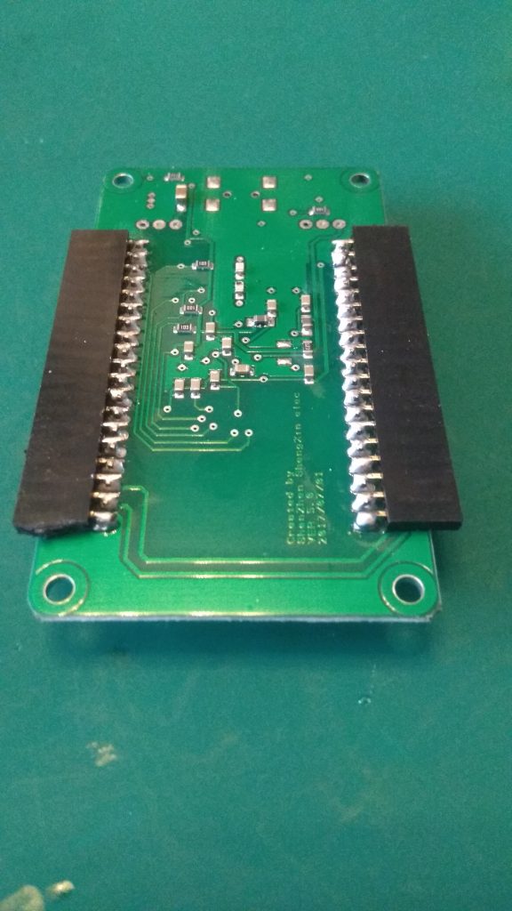
The Open source DSO-138 features support for 2 analog + 2 digital channels. A second analog channel requires hardware mods to the pcb.

DSO-138 with an additional digital channel

DSO-138: An open source firmware for DSO-138 O-Scope  

Summary

DSO-138 is an excellent piece of hardware based on ARM Cortex M3 core STM32F103 processor and sufficient for most beginner users. The stock firmware, while quite responsive, can use a few improvements. The main shortcoming which prompted the development of DLO-138 firmware is the inability to get waveform data into a computer for further analysis and the lack of a second channel. Engineers troubleshooting hardware issues need to mark reference points on waveform so having another analog or digital channel can greatly improve analysis. This firmware hopes to improve on these issues.
Features

  • Two analog channels
  • Two digital logic channels (SWDIO and SWDIO pins (PA13 and PA14) on board)
  • Serial port interface for captured waveform data
  • Trigger source selectable from Analog Channel 1 or Digital Channel
  • Option to use rotary encoder instead of + – and SEL switches
  • 2K sample depth

This firmware can be used on stock DSO-138 hardware as well. Select one of the pre-compiled binaries to suit the board. Follow the firmware upgrade instructions for DSO-138. At any time, you can reflash DSO-138 with JYE Tech provided firmware.

Cost

Extra features come at an additional cost. In the case of DLO-138, it is the loss of lowest timebase. Maximum sampling rate in DLO-138 is 20 µs/div instead of 10 µs/div. In the 20 µs/div range, firmware under-samples ADC channels, often reading same data twice. To use the second analog channel, analog front end has to be duplicated on a daughter board. On a stock hardware, this firmware can be used to provide two digital logic channels.

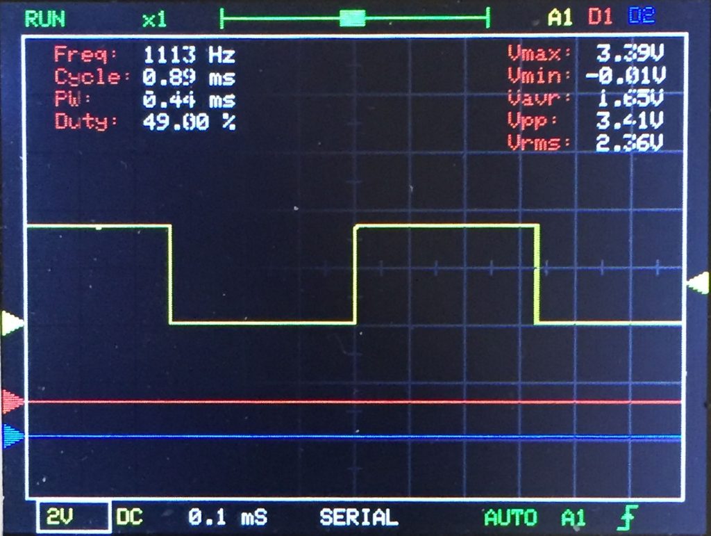
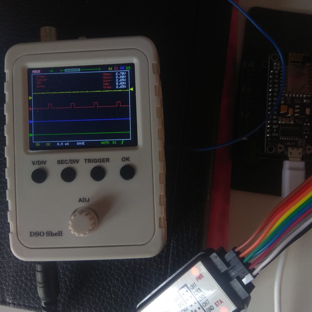
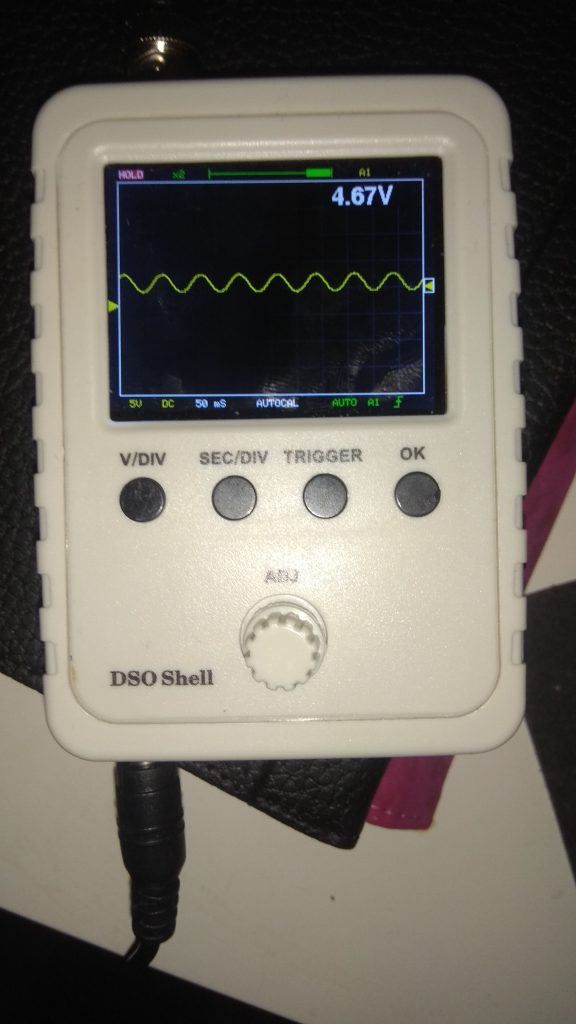
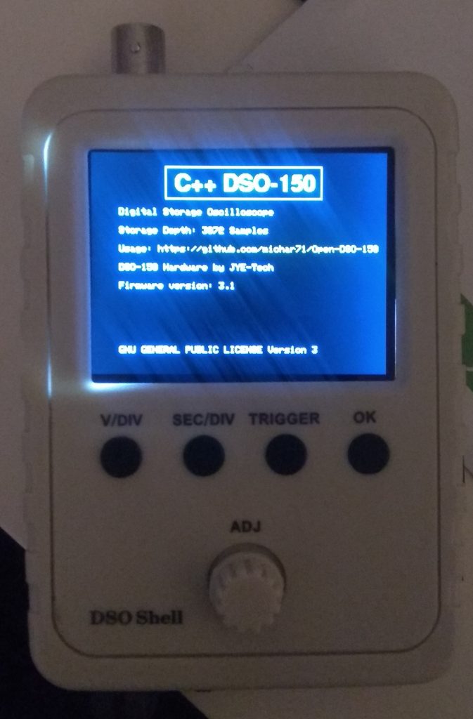
The Open source DSO-150 features support for 1 analog + 3 (yes 3) digital channels.

DSO-150 with 1 analog and 3 digital channels

DSO-150: An open source firmware for JYE Tech DSO-150 Digital Storage Oscilloscope

Summary

Complete rewrite of DSO-150 Firmware

  • No longer DSO-138 compatible (Sorry…)
  • Rewritten for Atollic trueSTUDIO (Yea… Real debugging)
  • Now using internal digital trigger through ADC IRQ (So trigger level can now be correlated to real voltage)
  • Lots of new features like voltage overlay, markers, auto cal

Features

  • Support 1 Analog and up to 3 Digital Channels
  • Trigger on rising/falling/both edges
  • Trigger on Analog, Digital 1,2,3 Signal
  • Single/Norm/Auto Trigger Mode
  • Exact trigger voltage
  • Serial Data Dump
  • Automatic Zero-Level Cal for all gain-stages
  • Voltmeter mode (Averaged over last 10 samples)
  • Signal Statistics Display
  • Cursors for Analog Signal
  • Load/Store Waveform to/from Flash
  • Zoom Out Display (See more data with full sampling Rate)
  • “Persistence” Mode
  • Variable Signal Size for Digital Signal Waveform
  • “loop” mode to scroll current input-values
  • AC/DC mode
  • 3K Sampling Depth
  • Buttons not blocked during sampling

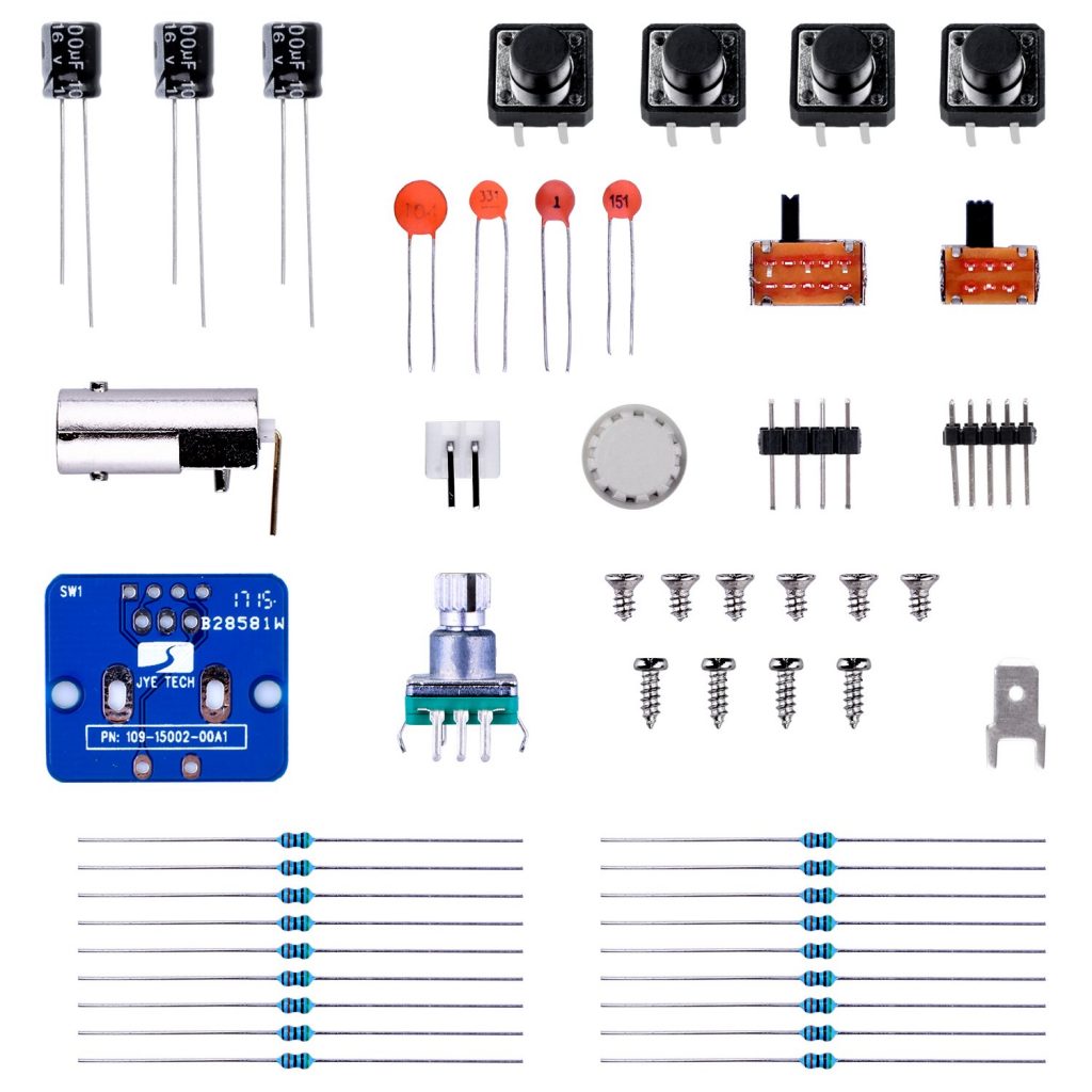
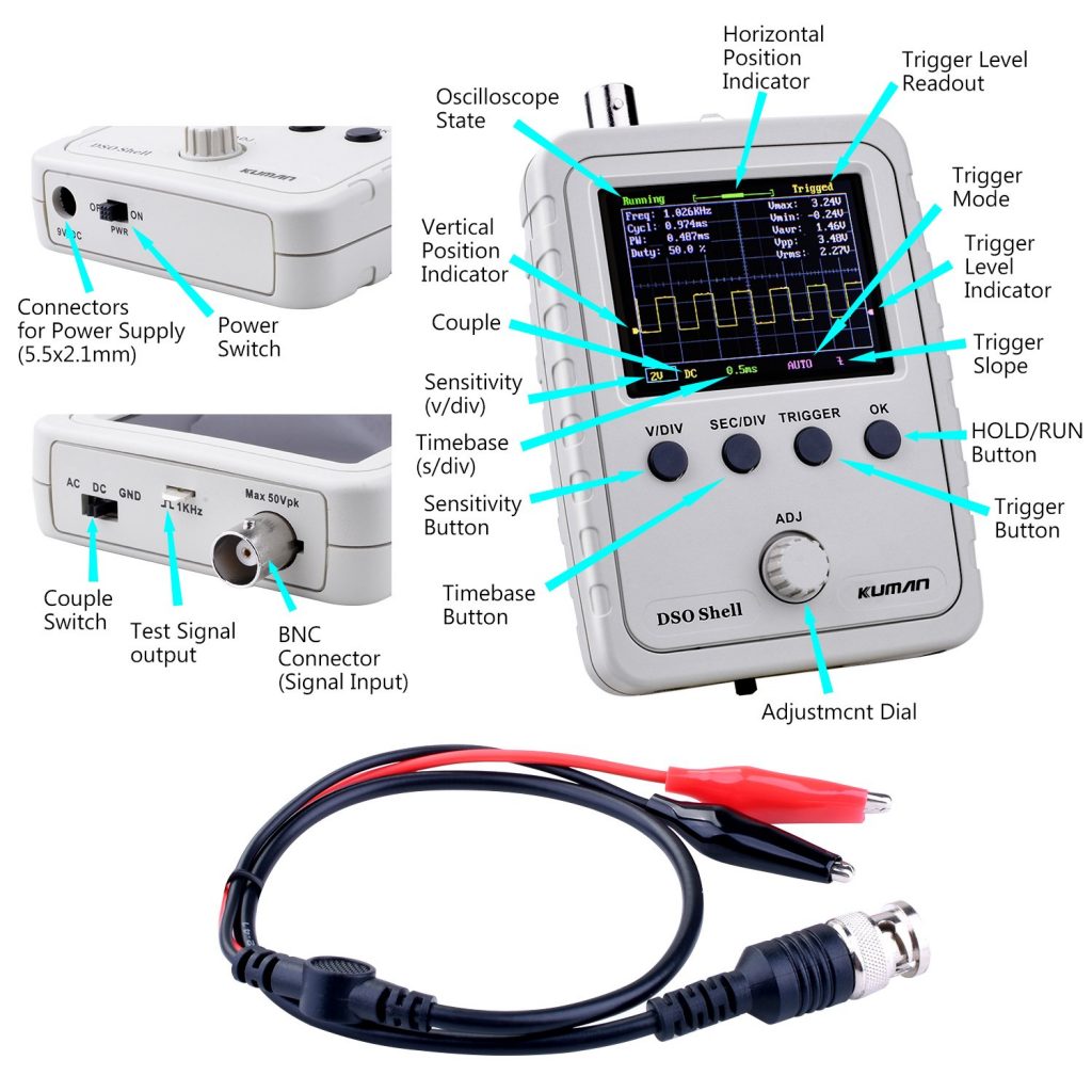
After discovering the availability of the enhanced firmware, I bit the bullet and decided to get a DSO-150. Not looking forward to doing that much soldering, I therefore chose yet another purchase option of DIY “pre-soldered, just pop everything into the case on arrival”.

The instructions of building and flashing the DSO-Firmware are included in the github page, but as things never go smoothly, I had to

  • Convert the built binary to HEX format

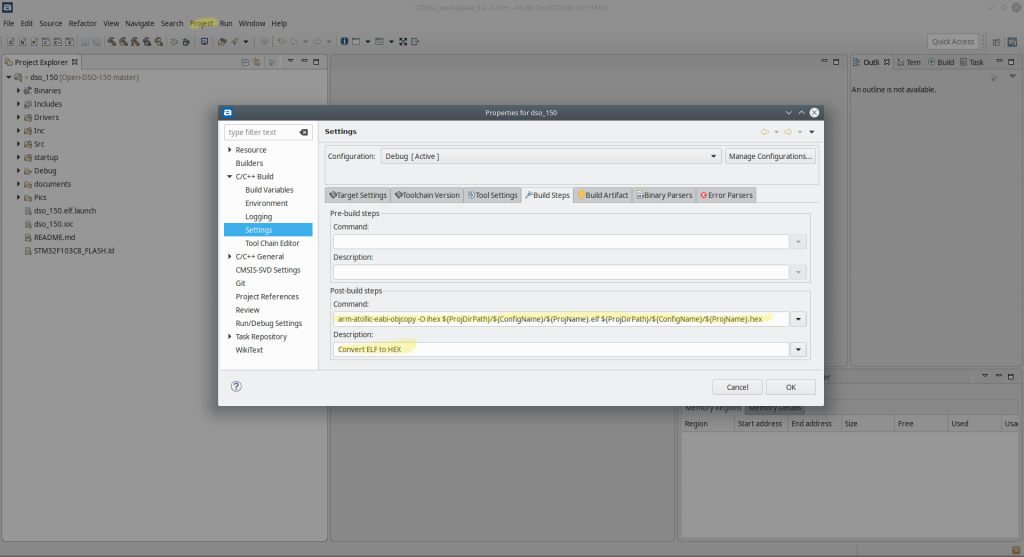
After building the project in TrueStudio you will be left with an ELF binary file. To be able to update the firmware the ELF file will have to be in HEX file format. This can be easily achieved by adding a post build step to the project.

The post build command is

and the post build description can be whatever you like, in my case

So now when you build the project you will end up with both an ELF file and a HEX file. The HEX file is what you will flash to the DSO.


  • Flashing the device.

I tried to flash the device via the on board USART1 with both Linux and Windows using the tools,

Download stm32flash with git.

  • FLASHER-STM32 (windows) – STM32 Flash loader demonstrator (UM0462) @ https://www.st.com/b/en/development-tools/flasher-stm32.html
    • DSO-150 flashing instructions – Flashing Guide

But the device was not recognised with the message,

No response from the target, Bootloader cannot be started

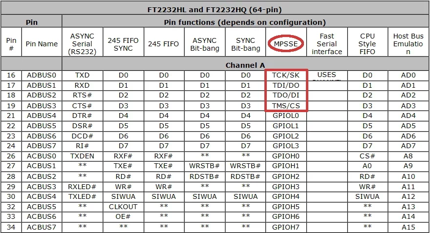
I eventually concluded that the required Serial bootloader was missing and gave up on UART flashing, deciding instead to flash via STLink/JTAG port. But not having an STLink handy, I decided to flash it with my FTDI FT2232H device and openocd on Linux.

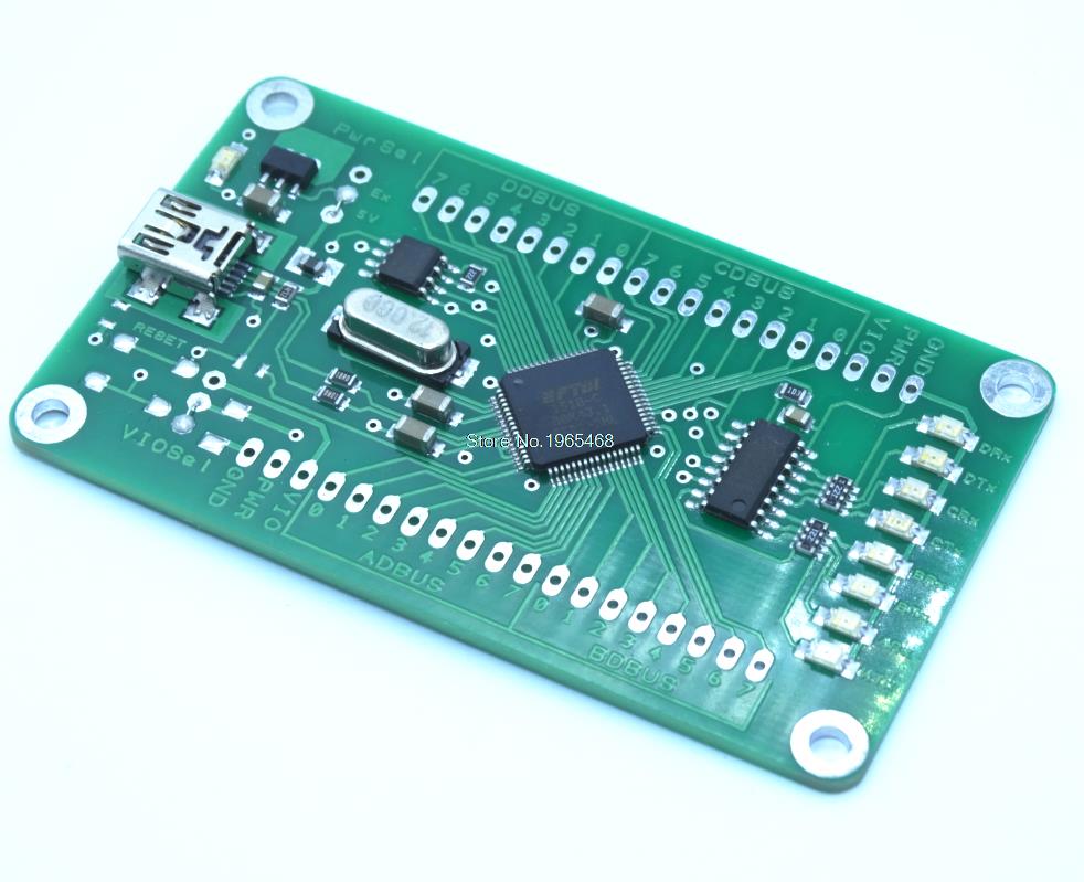
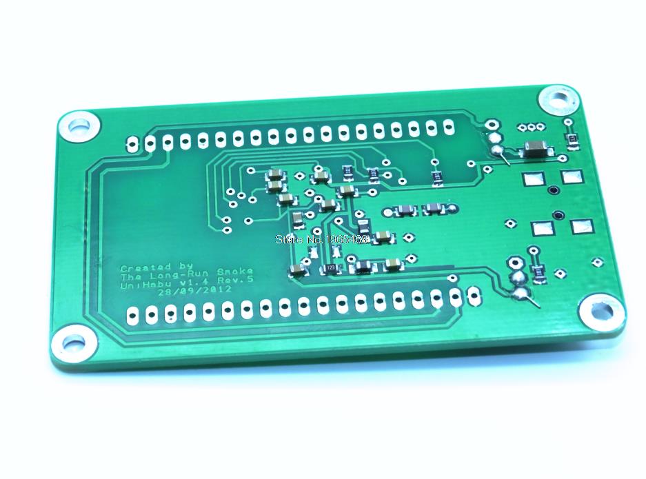
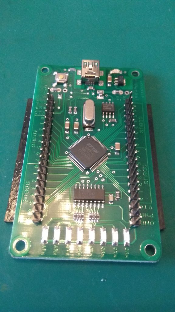
The FTDI device is readily available in various flavours at various outlets including Ebay, Aliexpress, and Amazon. Mine is shown below.

Plugging in the FT2232HL gives you a satisfying,

All About Circuits have a good primer on using and FTDI witth openocd @ https://www.allaboutcircuits.com/technical-articles/getting-started-with-openocd-using-ft2232h-adapter-for-swd-debugging/

I would follow their guide referring back here for DSO-150 specifics 🙂

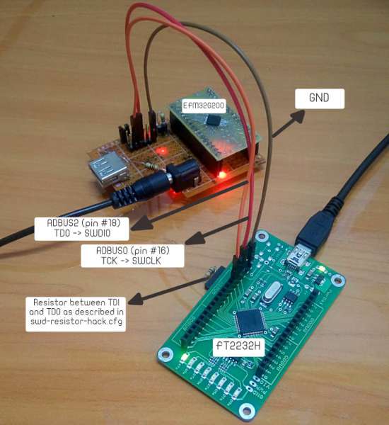
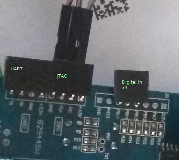
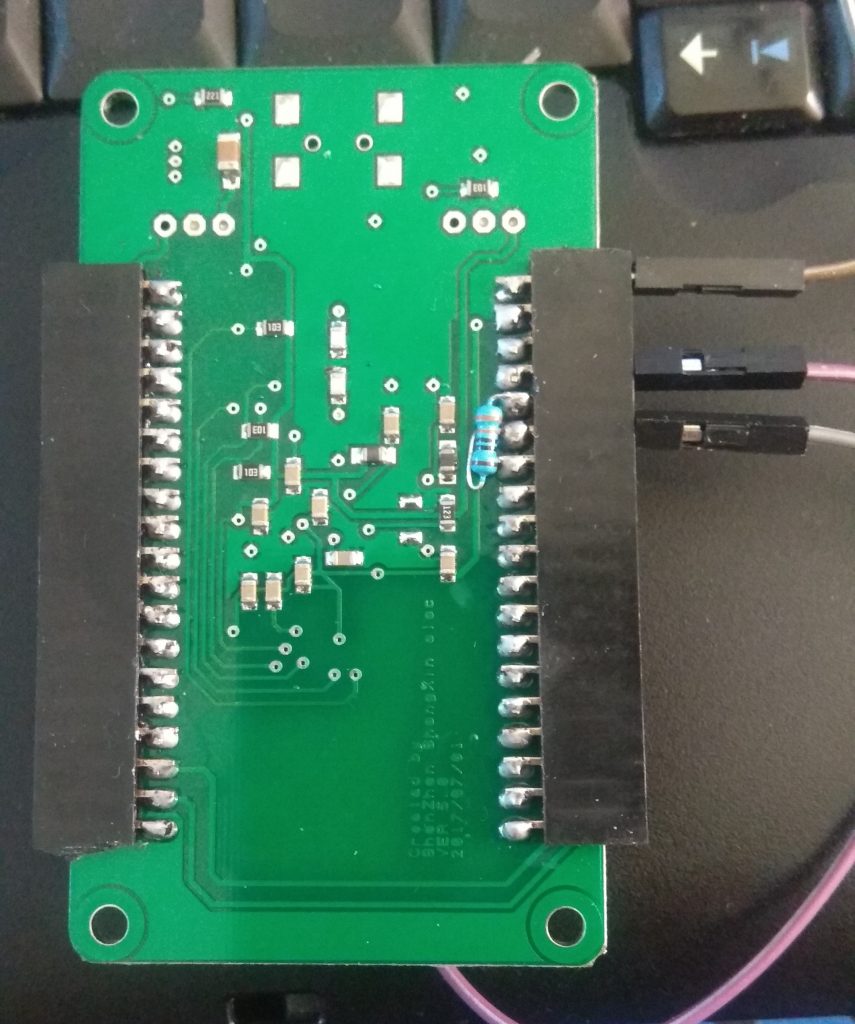
I soldered on some header pins to the FT2232HL and DSO-150.

Now the wiring was complete I installed openocd and moved on to setting up the configuration files required by openocd

  • /usr/share/openocd/scripts/interface/ftdi/myft2232hl.cfg

is the number from the dmesg log!

  • /usr/share/openocd/scripts/target/stm32f1x.cfg

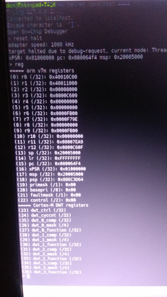
If you have wired up the FTDI FT2232H (or whichever) correctly then running openocd should give you,

I forgot to take notes at the time of flashing, but I remember having to unprotect the flash!

Update: This post describes in detail the process of flashing a STM32 Cortex M3 with openocd 🙂 https://jacobmossberg.se/posts/2017/01/10/using-openocd-flash-arm-cortex-m3.html

These are the commands I executed during the process of flashing.

Anyway the take away is that I got it flashed, but not via the UART, I had to use the JTAG port and the new digital inputs are fully functional.

DSO-150 User Instructions – User Guide

DSO-150 How to Upgrade Firmware (Official) – Flashing Guide

ESP-01S Relay Module V1.0

Overview

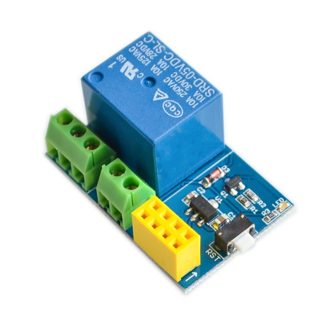
I picked up 10 of these modules (including the ESP-01s units) on Aliexpress for the purpose of controlling domestic AC powered equipment .e.g lights, fan heaters and such like.

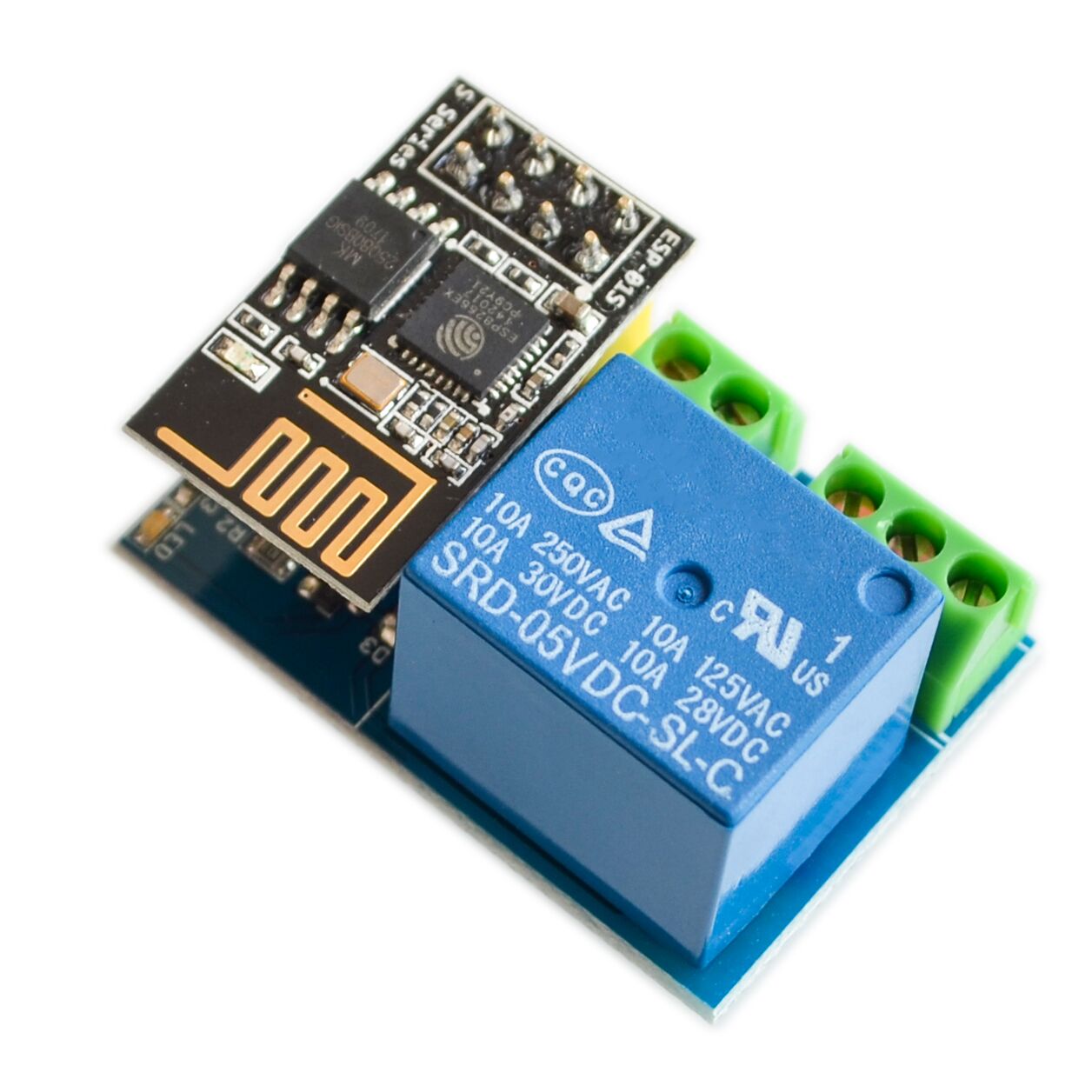
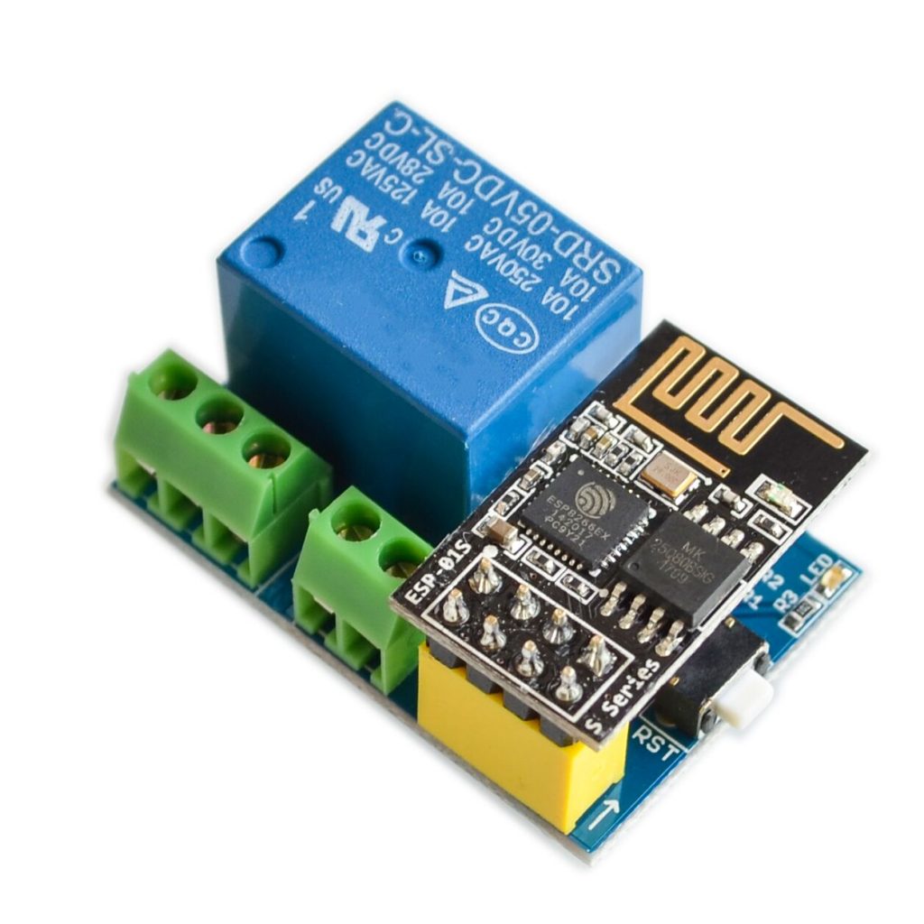
It is a compact little module that directly holds the esp-01s in an 8-pin female pin header. Features of note are

  • The Relay is a Songle SRD-05VDC-SL-C rated at 240V 10A. Datasheet
  • A 7002 mosfet for switching the relay via GPIO0. Datasheet
  • The Relay is activated via GPIO0.
  • GPIO2 is free for monitoring a sensor button, switch, thermostat etc..
  • A reset button.
  • The 5v power input is converted to a ESP8266 compatible output of 3.3v via a AMS1117 3.3v linear voltage regulator. Datasheet

Problems

The relay module’s design (albeit compact and aesthetically pleasing) does present a few problems detailed below –

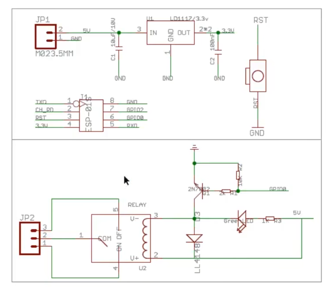
  1. The CH_PD pin is not pulled up to VCC and is left floating and as such the esp-01s module will never activate.
  2. The GPIO0 pin is pulled down to GND via resister R2. This means that the esp-01s module will start up in Flashing mode.
  3. The AMS1117 3.3v linear regulator. The problem with these is that when they fail they fail big and go short circuit feeding the (in this case 5v) input voltage straight through to the output pins. I managed to short one out while messing with the esp-01s CH_PD pin and now have a steady 5v-5v regulator on the Relay module and a dead esp-01s module.
    The Relay module can be rescued by replacing the AMS1117 3.3v regulator but the esp-01s has blinked it’s last LED.
    I have also fried AMS1117 5V regulators on breadboard power supplies as discussed in Breadboard power supply module destructive failure.

Fix

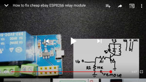
A helpful Youtube video can be found below.

How to fix cheap ebay ESP8266 relay module

To summarise the points raised in the video…

  • The fix for the GPIO0 problem is to simply remove the resister R2. This will stop it being pulled LOW on boot.
  • Connect the CH_PD pin to VCC pin either on the esp-01s or on the relay module. This will enable the esp-01 on boot.

The Kingst LA1002 Logic Analyser

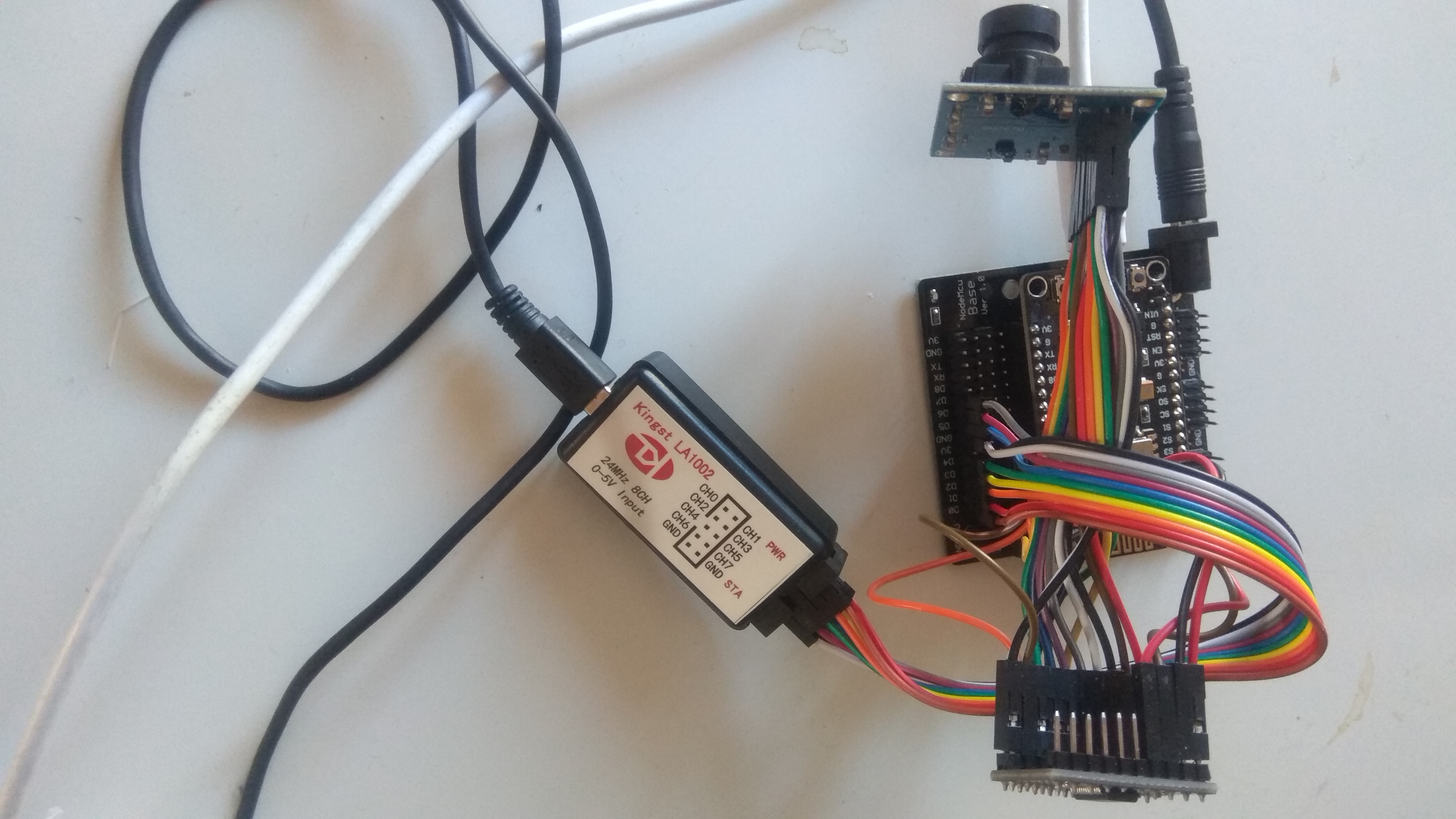
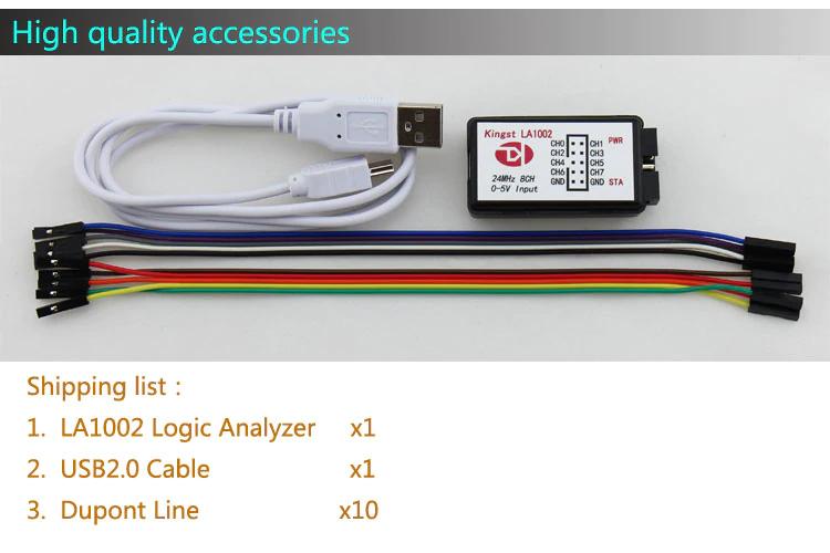
While playing with the ESP8266, ESP32, STM32 and OrangePIs, I decided it might be a good idea to invest in a logic analyser. I opted for a cheap Kingst LA1002 with a sampling rate of 24M @ 8channels. The product while still sold on Aliexpress does not seem to be available on their website.

ESP8266 and OV7670
Fun with an ESP8266 and OV7670 camera module

While I doubt that it can actually achieve the stated specifications the associated product blurb states

LA1002 is a logic analyzer product with high cost performance. It has 8 input channels and the sampling rate is up to 24M. Along with the PC software KingstVIS, 8 channels of digital signal could be sampled at the same time, and then they could be converted to digital waveform and displayed on the PC screen. The signal could be analyzed with many standard protocols, to get more straightforward communication data. It helps a lot in testing and analyzing digital system(MCU/ARM/FPGA, etc.), developing and debugging several communication programs, or monitoring and recording some digital signals for a long time.

Features

·Portable and lightweight
·Max sampling rate: 24M @ 8channels
·Large sampling depth and support compression
·Compatible USB2.0/3.0 interface
·Powerful software and easy to use
·Support online upgrade automatically

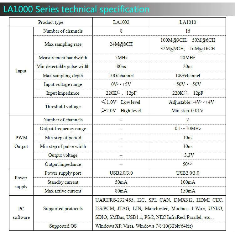
Specifications

·Input channels number: 8
·Max sampling rate: 24M
·Measurement bandwidth: 5M
·Min pulse width can be captured: 80ns
·Max sampling depth: 10G/channel
·Input voltage range: 0V ~ +5V
·Input impedance: 220KΩ, 12pF
·Threshold voltage: Low level < 1.0V, High level > 2.0V
·Standby current: 50mA
·Max operating current: 80mA
·Dimensions: 53mm * 28mm * 14mm
·Supported OS: Windows XP, Vista, Windows 7/8/10(32/64bit)

Supported standard protocols: UART/RS-232/485, I2C, SPI, CAN, DMX512, HDMI CEC, I2S/PCM, JTAG,
LIN, Manchester, Modbus, 1-Wire, UNI/O, SDIO, SMBus, USB1.1, PS/2, NEC InfraRed, Parallel, etc…

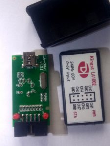
The LA1002 appears similar to the Saleae 8 channel logic analysers and is based around a Cypress CY7C68013A-56LTXC and may also be supported by Sigrok. The USB ID of the Cypress CY7C68013A-56LTXC can apparently be programmed/changed thereby emulating other “well known” devices.


I didn’t spend too much time investigating cloning LA1002’s USB ID to match the Salaea or using the Sigrok software as the Kingst supplied software (supporting Linux, Windows and Mac) seems more than adequate for my needs.

Linux version - Ubuntu Bionic
Linux version – Ubuntu Bionic

Supported Analysers
Supported Analysers


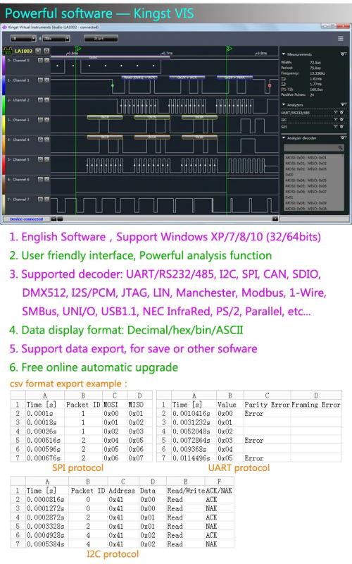
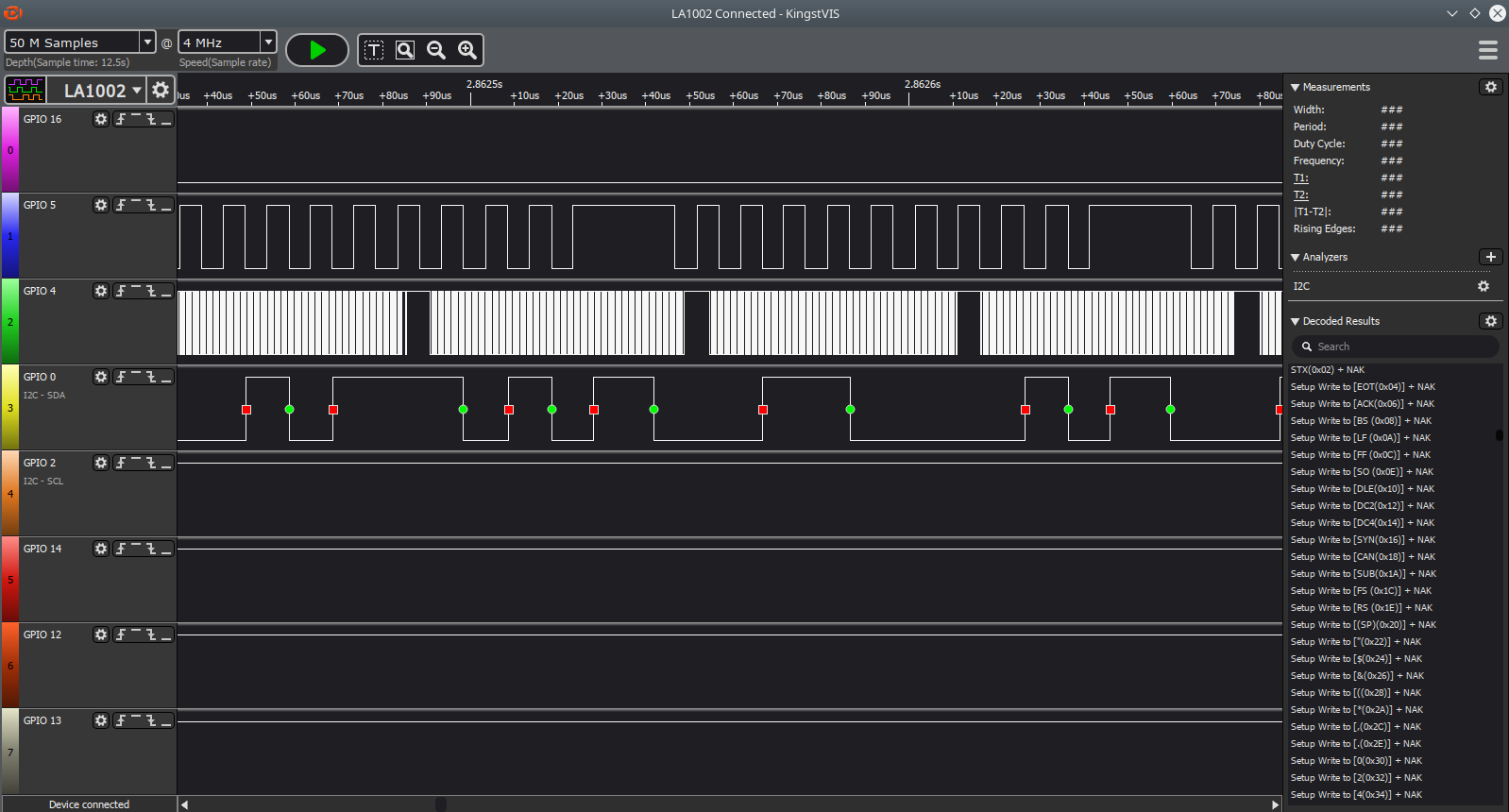
As can be seen in the screen grab, the KingstVIS software offers a nice range of protocol decoders and I find the dark shading of the User Interface quite easy on the eye.

More information on installation and operation of the LA1002 can be found in the User Guide
Qingdao Kingst Electronics Co., Ltd.
Web:www.qdkingst.com
E-mail:service@qdkingst.com